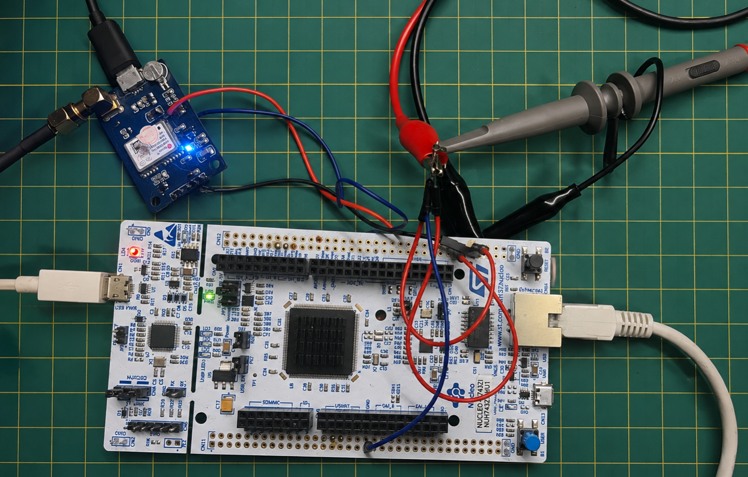
Current-code revision note
This revision supersedes the older 1 MHz / TIM3-TRGO timing description. The current firmware revision was checked against
main(5).c.The actual timing architecture is:
PA0 / 1 MHz ──► TIM5_CH1 ──► TIM5 counter / timestamp
PA3 / GNSS PPS ─────────────► TIM5_CH4 capture

PA6 / 1 MHz ──► TIM3_CH1 ──► reset ──► TIM3_CC4 ──► ADC1/2/3
In particular, TIM3 TRGO is not used for the ADCs. TIM5 does not generate the ADC sampling clock; it counts a separate external 1 MHz timing signal on PA0.
Overview
This project is the acquisition core of one unit in a distributed network of ground stations for VLF lightning direction finding. The same station architecture can be replicated across multiple sites, with GNSS providing the common timing reference and Ethernet carrying the raw measurements to a central processing host.
The unit captures three synchronized analog channels at 1 megasample per second (MSPS) and streams the raw samples via Ethernet/UDP to a Linux PC for storage and further signal processing. The same hardware architecture can be replicated across multiple stations and synchronized by GNSS timing.
The firmware uses an event-driven acquisition path: ADC DMA interrupts only publish completed blocks, while the main loop dequeues and transports them. This keeps network processing out of interrupt context and separates the timing-critical capture path from Ethernet handling.
Key specifications:
- 3 synchronized ADC channels — ADC1, ADC2, ADC3 driven from a shared 1 MHz trigger
- 1 MSPS per channel — 512-sample blocks every 512 µs
- Ethernet/UDP transport — each 3072-byte acquisition block is split into three UDP payloads kept below the MTU
- Timing metadata — each block carries a timer tick anchor and the most recent GNSS PPS reference for later time reconstruction
- Dropped-block detection — explicit block numbering makes acquisition gaps visible to the receiver
- Finite buffering — 128 blocks provide about 65.5 ms of acquisition buffering for transient transmission stalls
Motivation: Event-Driven Design
Traditional embedded firmware often couples data acquisition, buffering, and transmission in a monolithic interrupt handler. This approach introduces several problems:
- ISR bloat — Network stack code in interrupt context violates separation of concerns
- Unpredictable jitter — LwIP memory allocation or socket operations can delay ADC servicing
- Testing difficulty — Interrupt handlers are harder to reason about and instrument
This design inverts the dependency: ISRs only queue; the main loop dequeues and processes.
┌─────────────────┐
│  ADC DMA ISR    │
│  (every 512 µs) │  <- only enqueue completed block
└────────┬────────┘
         │
         ▼ (memory barrier)
    ┌─────────────────────┐
    │ Circular block queue │   (128 blocks × 3 KiB = 384 KiB)
    │ (head/tail indices)  │   (65.5 ms of acquisition buffer)
    └──────────┬──────────┘
              │
    ┌─────────▼──────────┐
    │  Main loop         │
    │  ADCCapture_       │
    │  Process()         │
    │                    │  <- dequeue block
    │  (unlimited time)  │  <- fragment & send UDP datagrams
    │                    │  <- LwIP housekeeping
    └────────────────────┘
The result is a small and testable acquisition path with explicit buffering and visible failure modes.
Hardware Setup
The system is built around a NUCLEO-H743ZI development board and off-the-shelf components:

Microcontroller & Clocking
- STM32H743ZI — 480 MHz Arm Cortex-M7
- TIM3 — external-clocked ADC trigger timer; receives a 1 MHz signal on PA6 / TIM3_CH1, resets its counter on each falling edge, and generates TIM3_CC4 at a fixed timer-clock offset
- ADC1/ADC2/ADC3 are triggered directly by TIM3_CC4
- TIM3 TRGO is not used
- TIM5 — 32-bit external counter used as the long-term sample-time reference
- Counts a separate external 1 MHz signal on PA0 / TIM5_CH1
- Uses TIM5_CH1 directly for the external clock; the previous indirect TI2 routing is removed
- Captures GNSS PPS on PA3 / TIM5_CH4
- System clock — 480 MHz; TIM3 timer clock is configured/used at 240 MHz in the current firmware
Analog Acquisition
- ADC1, ADC2, ADC3 — Each running in externally triggered mode
- Shared TIM3_CC4 trigger
- ADC trigger source is
ADC_EXTERNALTRIG_T3_CC4, rising edge - Circular DMA, 512-sample blocks
- Half-transfer + complete-transfer interrupts
- DMA — current firmware uses DMA1 streams for ADC1/ADC2/ADC3; acquisition buffers are placed in DMA-accessible SRAM
Networking
- LAN8742A PHY — on-board Ethernet interface
- LwIP TCP/IP stack — UDP endpoint at 192.168.7.2:5000
- Point-to-point link — direct Ethernet cable to acquisition PC (192.168.7.1)
Timing
- u-blox NEO-M8T GNSS receiver — provides PPS pulse and RTC
- 3.3 V LDO — clean power for sensitive GNSS hardware
- External 1 MHz timing inputs:
- PA0 / TIM5_CH1 — external 1 MHz counter reference for TIM5
- PA6 / TIM3_CH1 — external 1 MHz sampling reference for the ADC trigger timer
- GNSS PPS — PA3 / TIM5_CH4 for hardware capture
Firmware Architecture
Layer 1: ADC & DMA Acquisition
File: adc_capture.c — DMA circular buffers + interrupt queuing
#define ADC_BLOCK_SAMPLES    512
#define DAQ_CHANNEL_COUNT    3
#define DAQ_BLOCK_PAYLOAD    (512 * 3 * 2)  // 3072 bytes
Three 16-bit circular DMA buffers (one per ADC) are continuously filled. When a DMA half-transfer completes, both ADC and timer state are captured atomically:
void HAL_ADC_ConvHalfCpltCallback(ADC_HandleTypeDef *hadc)
{
    if (hadc->Instance == ADC1) {
        OnBlockBoundary(0);  // offset = 0 (first half)
    }
}

void HAL_ADC_ConvCpltCallback(ADC_HandleTypeDef *hadc)
{
    if (hadc->Instance == ADC1) {
        OnBlockBoundary(1);  // offset = 512 (second half)
    }
}
Layer 2: Event Queueing
Inside OnBlockBoundary():
- Check queue headroom — If the queue is full, increment dropped-block counter and return
- Collect metadata:
- Block number (incremented per half-transfer)
- TIM5 tick of the first sample in this block
- Latest GNSS PPS tick (from
TickCounter) - PPS sequence counter
- Interleave samples — Deinterleave from three separate ADC buffers into wire format:
ch1[0], ch2[0], ch3[0], ch1[1], ch2[1], ch3[1], ... - Publish with memory barrier — Update queue head index (DMB ensures visibility)
The operation is kept short; no network code runs in ISR context.
Layer 3: Main Event Loop
File: main.c — Minimal main loop
while (1) {
    MX_LWIP_Process();       // ARP, link state, incoming packets
    ADCCapture_Process();    // Dequeue & transmit
    DebugLog_Poll();          // current firmware debug/statistics polling
}
Layer 4: UDP Transmission
File: adc_capture.c — ADCCapture_Process() function
The completed block at the queue tail is fragmented and sent:
- Fragment into UDP payloads of at most 1400 bytes (keeps the IP packet below the usual 1500-byte Ethernet MTU)
- 3072 bytes → 3 datagrams (1400 + 1400 + 272 bytes of sample payload)
- Send the fragments from the main loop so the acquisition ISR remains isolated from the network stack
- If LwIP returns ERR_MEM → stop and retry next loop iteration
- On completion → advance tail index and move to next block
In the tested configuration, the 6 MB/s sample stream is well below the 100 Mbit/s Ethernet link capacity; the remaining headroom is useful for protocol overhead and future processing.
Wire Protocol
UDP Datagram Format
All multi-byte fields are little-endian on the wire.
typedef struct {
    uint16_t magic;              // 0xA5D1
    uint8_t  version;            // 1
    uint8_t  header_size;        // 40 bytes
    uint8_t  flags;              // reserved, 0
    uint8_t  fragment_index;     // 0 .. fragment_count-1
    uint8_t  fragment_count;     // 3
    uint8_t  reserved0;
    uint32_t block_number;       // increments every 512 µs
    uint64_t tick_anchor;        // TIM5 tick of first sample
    uint64_t pps_anchor_tick;    // latest GNSS PPS tick
    uint32_t pps_seq;            // PPS sequence counter
    uint16_t samples_per_channel;// 512
    uint16_t payload_offset;     // byte offset in raw block (0, 1400, 2800)
    uint16_t payload_bytes;      // bytes in this fragment
    uint16_t reserved1;
} daq_udp_header_t;  // 40 bytes
Payload: 0–1400 bytes of interleaved ADC samples (uint16_t per channel per sample).
Reconstruction on PC
The Python receiver (daq_udp_receiver.py):
- Reassembles fragments — tracks which fragments have arrived for each block
- Validates headers — magic, version, alignment
- Writes to binary file — raw interleaved samples for offline analysis
- Reports gaps — block number discontinuities reveal Ethernet backpressure
python3 daq_udp_receiver.py --iface 192.168.7.1 --output capture.bin
Timing & Synchronization
This is the heart of the system. A distributed lightning direction-finding network needs the three channels within a station to share the same sampling clock, while GNSS PPS provides an absolute time reference that can be compared across stations.
ADC Trigger: TIM3_CC4 @ 1 MHz
Requirement: All three ADCs must sample synchronously at 1 MHz.
Current implementation: TIM3 is not a free-running 1 MHz generator and it does not use TRGO for the ADC trigger.
The current firmware configures:
- PA6 / TIM3_CH1 as an external 1 MHz input;
- TIM3 in Slave Reset mode with
TIM_TS_TI1FP1; Prescaler = 0;ARR = 0xFFFF;- TIM3 timer clock = 240 MHz in the current clock configuration;
- CCR4 = 1;
- ADC1/ADC2/ADC3 external trigger source =
ADC_EXTERNALTRIG_T3_CC4; - ADC trigger edge = rising.
Operation is therefore:
External 1 MHz input
        │
        ▼
 PA6 / TIM3_CH1
        │
        ▼
   TI1FP1 / Reset
        │
        ├── CNT := 0 on each falling edge
        │
        ▼
     CNT = 1
        │
        ▼
   TIM3_CC4 event
        │
     ┌──┼──┐
     ▼  ▼  ▼
   ADC1 ADC2 ADC3
With a 240 MHz TIM3 clock and CCR4 = 1, the compare point is one timer tick (~4.17 ns) after the timer reset point. This is the timer-domain offset between reset and CC4; it is not the total physical delay or jitter from the external PA6 edge to ADC sampling. The 1 MHz sample rate comes from the external PA6 signal, not from ARR and not from TIM3 TRGO.
The current code explicitly sets:
hadc1.Init.ExternalTrigConv = ADC_EXTERNALTRIG_T3_CC4;
hadc1.Init.ExternalTrigConvEdge = ADC_EXTERNALTRIGCONVEDGE_RISING;
and the equivalent trigger configuration is used for ADC2 and ADC3.
Important: the current firmware therefore has two separate 1 MHz timing inputs:
- PA0 → TIM5 for the long-term tick counter;
- PA6 → TIM3 → CC4 → ADCs for sampling.
If PA0 and PA6 are physically driven by the same 1 MHz source, they are frequency-related externally, but the firmware treats them as separate timer inputs.
Tick Counter: Extended 64-Bit TIM5 Timebase
TIM5 is a 32-bit counter used as the acquisition timebase. In the current firmware it is clocked directly from an external 1 MHz signal on PA0 / TIM5_CH1.
With a 1 MHz external clock:
$$T_{overflow} = \frac{2^{32}}{1 \times 10^6} = 4294.967 \text{ seconds} \approx 71.58 \text{ minutes}$$The current configuration is:
htim5.Init.Prescaler = 0;
htim5.Init.CounterMode = TIM_COUNTERMODE_UP;
htim5.Init.Period = 4294967295;
htim5.Init.ClockDivision = TIM_CLOCKDIVISION_DIV1;

sSlaveConfig.SlaveMode = TIM_SLAVEMODE_EXTERNAL1;
sSlaveConfig.InputTrigger = TIM_TS_TI1FP1;
sSlaveConfig.TriggerPolarity = TIM_INPUTCHANNELPOLARITY_FALLING;
Thus TIM5 counts the selected falling edges of TI1FP1, i.e. the direct TIM5 CH1 input on PA0.
The current firmware deliberately does not use the older indirect-TI2 routing. In particular:
PA0 / TIM5_CH1
       │
       ▼
     TI1FP1
       │
       ▼
TIM5 External Clock Mode 1
       │
       ▼
    TIM5->CNT
TIM5 uses an external 1 MHz timing reference on PA0; it does not generate the ADC sampling clock.
The timer overflow is extended in software to form a longer-running timestamp. TickCounter_Init() is called before ADCCapture_EthernetInit(), because acquisition initialization takes an initial tick through TickCounter_Now().
PPS Capture: Hardware Timestamp Latch
The GNSS NEO-M8T provides a 1 PPS signal to PA3 / TIM5_CH4.
The current TIM5 configuration uses ordinary input capture on Channel 4:
GNSS PPS
   │
   ▼
PA3 / TIM5_CH4
   │
   ▼
TIM5 input capture
   │
   ▼
captured TIM5 counter value
The capture is performed by the timer peripheral, so the timer value is latched at the PPS edge rather than being measured by software after interrupt latency.
Current timing resolution: one TIM5 tick corresponds to the external PA0 timing frequency, which is 1 µs per tick at 1 MHz.
Therefore the current firmware does not have the 250 ns/tick resolution described by the older 1 MHz design.
From Ticks to UTC Time
Each acquisition block carries:
blk->meta.tick_anchor
blk->meta.pps_anchor_tick
blk->meta.pps_seq
tick_anchor is based on the TIM5 timebase, while pps_anchor_tick records the latest known PPS reference.
For the current firmware, the nominal TIM5 reference is 1 MHz:
timer_hz = 1_000_000.0
tick_period = 1e-6  # 1 µs
Once a PPS event is associated with a known UTC second, the receiver can use the TIM5 tick difference to reconstruct relative sample timing and attach UTC labels.
The exact UTC reconstruction implementation remains dependent on the current tick_counter/GNSS integration code; UART4 NMEA parsing is still a planned integration step.
Multi-Channel Phase Coherence
All three ADCs use the same TIM3_CC4 hardware trigger event:
PA6 1 MHz
   │
   ▼
TIM3 CH1 / reset
   │
   ▼
TIM3 CC4
 ┌─┼─┐
 ▼ ▼ ▼
A1 A2 A3
Therefore the three ADC peripherals are sample-synchronous at the 1 MHz acquisition rate by construction of the common trigger.
The remaining absolute channel-to-channel skew is not assigned a numerical value here; it should be measured experimentally because ADC internal timing, analog path delays, and PCB routing can contribute to the physical skew.
For the current firmware, TIM5 is not the ADC trigger. TIM5 provides the separate timestamp counter.
Clock Discipline Strategy (Future)
The current firmware uses external 1 MHz timing for both timing subsystems, but through separate inputs:
- PA0 → TIM5 counter;
- PA6 → TIM3 → ADC trigger.
A future timing-discipline layer can compare TIM5/PPS intervals against the expected 1,000,000 ticks per second:
uint64_t expected_interval = 1_000_000;
uint64_t actual_interval = pps_tick[i] - pps_tick[i-1];
int64_t error = actual_interval - expected_interval;
Long-term frequency characterization, oscillator discipline, and Allan-variance logging remain future work.
Performance Characteristics
Throughput
- Per block: 3072 bytes every 512 µs = 6.000 MB/s
- Per UDP packet: up to 1400 bytes of sample payload plus the application header and network overhead
- Ethernet payload utilization: 6.000 MB/s = 48 Mbit/s, or about 48% of a 100 Mbit/s link before protocol overhead
Latency
- A complete 512-sample block represents 512 µs of acquisition time before it can be transmitted as a block.
- The direct Ethernet link showed an average ICMP round-trip time of about 0.516 ms in the validation run.
- Application-level end-to-end latency was not independently characterized in this test, so it is not assigned a single numeric value here.
Buffering
- Circular queue: 128 blocks × 3072 bytes = 393,216 bytes (384 KiB)
- At 1 MSPS: 512 samples/block = 512 µs per block
- Buffer duration: 128 × 512 µs = 65.536 ms
- Purpose: the queue provides finite buffering for transient transmission stalls
Dropped Blocks
If Ethernet fully stalls (e.g., link down), the queue fills:
- A newly completed block is not enqueued once the queue is full
- Block number still advances, so the receiver can detect the missing block
- No silent corruption — receiver explicitly detects the gap
Known Good Configuration
The project includes a known-good hardware configuration that documents the tested prototype setup:
- Ethernet configuration — RMII Ethernet using the NUCLEO-H743ZI on-board PHY
- ADC configuration — three independent ADC peripherals with timer-triggered conversions
- Clock tree — 480 MHz system clock; external 1 MHz timing is used by TIM3 for the ADC trigger and by TIM5 for the timestamp counter
- Timer inputs — PA0 / TIM5_CH1 for the TIM5 counter; PA6 / TIM3_CH1 for the ADC trigger timer; PA3 / TIM5_CH4 for GNSS PPS
- DMA routing — circular ADC DMA buffers placed in DMA-accessible SRAM
- UARTs — USART3 for debug logging; UART4 reserved for future GNSS NMEA input
GNSS Integration: u-blox NEO-M8T
The NEO-M8T is used as the GNSS timing source for:
- 1 PPS output — provides a one-second timing reference for the acquisition unit
- NMEA output — GGA/RMC data can be used to bind PPS events to UTC
- Independent station timing — the same GNSS timing architecture can be replicated across multiple ground stations
Hardware Connection
NEO-M8T Breakout
    ├─ VCC → 3.3 V LDO (mean-well RS-15-5 + STM32 LDO)
    ├─ GND → chassis ground
    ├─ TX  → UART4 RX (PB9)        [NMEA output, 9600 baud]
    ├─ RX  → UART4 TX (PB8)        [future: commands]
    ├─ PPS → PA3 (TIM5 CH4)        [hardware capture]
    └─ ANT → active GPS antenna    [1575.42 MHz]
The GNSS receiver is supplied through a dedicated regulated rail and local decoupling. The exact power-integrity budget is hardware-dependent and should be verified on the final field node, especially when the analog front end and Ethernet PHY share the same supply system.
UART4: NMEA Receiver (Future Phase)
Currently placeholder; next phase will parse GGA and RMC sentences:
$GPRMC,123519,4807.038,N,01131.000,E,022.4,084.4,230394,003.1,W*6A
         ^^^^^^                                        ^^^^^^
         hhmmss (UTC)                                 date (ddmmyy)

$GPGGA,123519,4807.038,N,01131.000,E,1,08,0.9,545.4,M,46.9,M,,*47
         ^^^^^^                          ^^  ^^
         hhmmss                          #sat HDOP
Parsing strategy:
- UART4 interrupt handler — copy incoming bytes to circular buffer
- Main loop polling — extract complete sentences
- UTC offset calculation — from first GGA with fix (occurs 1–10 seconds after PPS sync)
- Timestamp reachback — apply UTC to all samples since last PPS
PPS Sync: Absolute Time Anchor
The GNSS receiver provides a 1 PPS timing pulse aligned to UTC seconds; the exact pulse polarity and width are configured at the receiver and matched to the TIM5 input-capture edge.
UTC second N    |  UTC second N+1
                ▼                ▼
─────────────┐     ┌───────────┐
             └──┬──┘           └──┬──
            PPS pulse          PPS pulse
            (configured edge       (configured edge
             captured by TIM5)       captured by TIM5)
Timing workflow:
- Boot: TIM5 free-runs, records tick_anchor for each ADC block
- PPS arrives (event N):
- TIM5 CH4 capture → captured timer value at the PPS edge
- ISR reads the TIM5 CH4 capture value (
CCR4), updatespps_anchor_tickandpps_seq - All blocks queued after this moment include the new PPS reference
- Later, GGA fix arrives:
- Extract UTC time from sentence
- Compute the UTC offset using the current 1 MHz TIM5 timebase
- Retroactively timestamp all blocks since last PPS
- Steady state:
- Each block carries its own tick_anchor
- Receiver computes block UTC from the PPS anchor and the 1 MHz TIM5 tick difference
Offline Signal Processing Pipeline
The receiver PC writes raw 16-bit interleaved samples to disk. A NumPy post-processor then:
1. Block Reconstruction
with open('capture.bin', 'rb') as f:
    raw = np.frombuffer(f.read(), dtype='<u2')  # little-endian uint16

# Reshape from flat array to (n_samples, 3_channels)
samples = raw.reshape(-1, 3)
ch1, ch2, ch3 = samples[:, 0], samples[:, 1], samples[:, 2]
2. Calibration
Account for ADC zero offset (typically 2048 for 12-bit SAR centered around 1.65V):
adc_vref = 3.3  # volts
adc_bits = 12   # nominal
adc_offset = 2048  # measure from zero-input ADC samples

voltage = (samples - adc_offset) * (adc_vref / (2**adc_bits))
3. Time-Delay-of-Arrival (TDOA) Processing
For a distributed direction-finding implementation, the exact geometry depends on the antenna arrangement and station spacing. The acquisition unit itself is agnostic to that geometry and simply preserves the three time-aligned channels for downstream processing.
Cross-correlation between channel pairs gives sample-level time delay:
corr = np.correlate(ch1 - ch1.mean(), ch2 - ch2.mean(), mode='full')
max_lag = np.argmax(np.abs(corr)) - (len(ch1) - 1)
time_delay = max_lag / 1_000_000  # seconds

# The subsequent direction calculation depends on the actual
# antenna geometry, baseline, propagation model, and calibration.
4. Frequency Content Analysis
from scipy.fft import fft, fftfreq

# Compute PSD for each channel
n_fft = 4096
freq = fftfreq(n_fft, 1e-6)[:n_fft // 2]  # µs sampling period
psd1 = np.abs(fft(ch1[:n_fft]))**2 / (1_000_000 * n_fft)  # V²/Hz

plt.semilogy(freq, psd1)
plt.xlabel('Frequency (Hz)')
plt.ylabel('PSD (V²/Hz)')
plt.xlim(1e3, 30e3)  # 1–30 kHz VLF band
plt.show()
Dropped Blocks & Ethernet Backpressure
The circular queue is intentionally finite (128 blocks × 3 KiB). When ADC DMA outruns Ethernet transmission:
Example scenario:
  - ADC produces 512 samples/512 µs = 1 block per 512 µs
  - Network stalls (link renegotiation, host scheduling, or receive-side backpressure)
  - Queue gradually fills at the acquisition rate of 6 MB/s

  When the 128-block queue is full:
              -> new block cannot be enqueued
              -> dropped_blocks++
              -> block_number continues incrementing
              -> receiver later detects the missing block number
Receiver detects the gap:
blocks_received = [10, 11, 12, 15, 16, ...]  # blocks 13 and 14 missing
gap_size = 15 - 12 - 1 = 2  # dropped 2 blocks

print(f"Lost {gap_size * 512} samples ({gap_size * 0.512} ms)")
This design is preferable to silent corruption. The dropped blocks prove the system is under backpressure, so the user knows to:
- Reduce ADC sample rate
- Use a faster Ethernet link (1 Gbps vs 100 Mbps)
- Move PC-side processing to dedicated FPGA or second STM32
Power Consumption & Thermal
The current NUCLEO-based prototype was measured at approximately 620 mA at 3.3 V, or about 2 W for the node in the tested laboratory configuration. This is a prototype-level figure rather than a final field-station power budget.
For deployment, the final power budget must include the analog front end, GNSS receiver, Ethernet PHY, power-conversion losses, enclosure conditions, and any storage or backup power. Battery runtime should be calculated from total energy (Wh) and measured system power rather than from nominal cell capacity alone.
Thermal behavior of the prototype has only been evaluated in the laboratory. Enclosure and ambient-temperature testing remain part of the field-station engineering work.
Debug & Instrumentation
UART3: Serial Console (115200 8N1)
Prints block statistics every 1 second:
Blocks: 12345 | Dropped: 0 | UDP sent: 37035 | Errors: 0 | Rate: 6.008 MB/s
Blocks: 12721 | Dropped: 0 | UDP sent: 38163 | Errors: 0 | Rate: 6.009 MB/s
USB Virtual COM Port (USBD_CDC)
Available but not used in current firmware (resource for future NMEA input or command interface).
Online Monitoring
Python script monitors UDP stream in real-time:
python3 daq_udp_receiver.py \
    --iface 192.168.7.1 \
    --output capture.bin \
    | tee log.txt
Output shows dropped-block detection in real-time:
blocks=      100 missing=        0 bad=      0 fragments=      300 rate=  6.009 MB/s
blocks=      200 missing=        0 bad=      0 fragments=      600 rate=  6.008 MB/s
blocks=      487 missing=        3 bad=      0 fragments=     1461 rate=  6.001 MB/s  <- loss event
blocks=      500 missing=        3 bad=      0 fragments=     1500 rate=  6.000 MB/s
Software Stack
Bare-Metal Core
- STM32CubeMX-generated HAL — GPIO, clock, DMA, ADC, UART, USB
- Custom firmware — adc_capture.c (event queueing), tick_counter.c (PPS timing), debug_log.c (console)
- FreeRTOS-free — the current design keeps scheduling simple and avoids introducing RTOS task scheduling into the capture path
Middleware
- LwIP — lightweight TCP/IP stack used for UDP unicast transport
- STM32 USB Device Library — CDC for debug (future NMEA input)
- CMake + arm-none-eabi-gcc — reproducible cross-compilation
PC-side
- Python 3.7+ — daq_udp_receiver.py (UDP socket, block reassembly, file I/O)
- NumPy 1.20+ — array operations, reshape, FFT
- SciPy — signal processing (correlate, fft)
- Matplotlib — real-time plotting of PSD, TDOA results
Next Steps
Planned Additions
Complete GNSS integration
- Parse NMEA output from u-blox NEO-M8T on UART4
- Attach UTC timestamp to each block
- Long-term frequency drift logging
Advanced Timing
- Disciplined local oscillator (DLO) using PPS
- Log frequency error and trending data
- Enable day-long measurement campaigns with sub-ppm drift
Direction-of-Arrival (DoA) Processing
- Offline spatial signal processing on captured blocks
- Time-delay-of-arrival (TDOA) triangulation
- Bearing accuracy benchmarks
Remote Command Interface
- TCP server for runtime gain adjustment
- Frequency sweep automation
- Ethernet-based trigger control
Validation & Measured Results
Hardware Proof-of-Life Test
Setup: Three channels looped back through preamp box, Hantek DSO2D10 oscilloscope monitoring output.

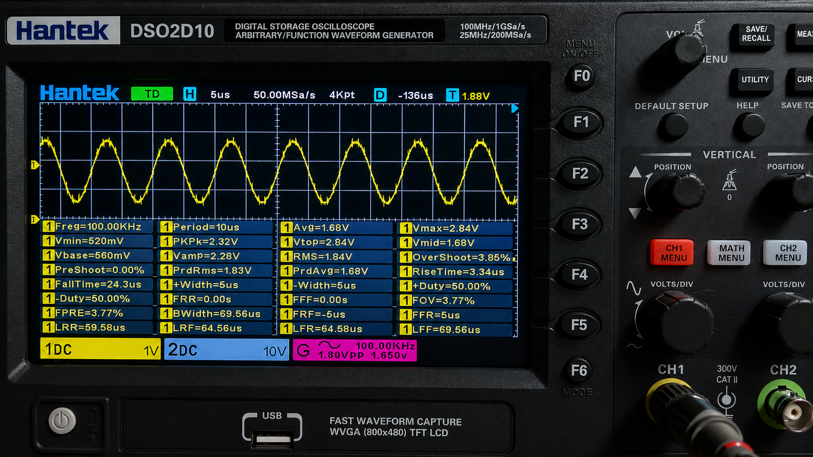
From oscilloscope capture:
- Frequency: 100 kHz sine
- Period: 10 µs
- Observed waveform: clean sine at the oscilloscope test point
- Hantek measurements:
- Vmin = 520 mV, Vmax = 2.84 V, Vbase = 560 mV
- Vamp = 2.28 V, Vavg = 1.68 V
- PreShoot = 0%, OverShoot = 3.85%, RMS = 1.84 V
This confirms that the analog test path can pass the 100 kHz verification signal without visible waveform failure at the monitored test point. It is a lab proof-of-life measurement rather than a complete characterization of the final VLF analog front end.
Ethernet Packet Capture

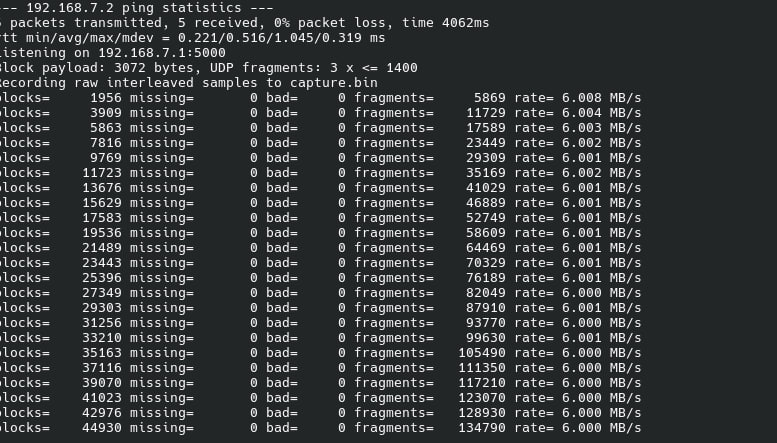
From ping statistics:
192.168.7.1 ping 192.168.7.2
5 packets transmitted, 5 received, 0% packet loss, time 4062ms
rtt min/avg/max/mdev = 0.221/0.516/1.045/0.319 ms
This confirms:
- Point-to-point Ethernet link is up and stable
- Round-trip latency ~0.5 ms (excellent for UDP streaming)
- No ICMP packet loss in the shown idle-link test
ADC Waveform Capture

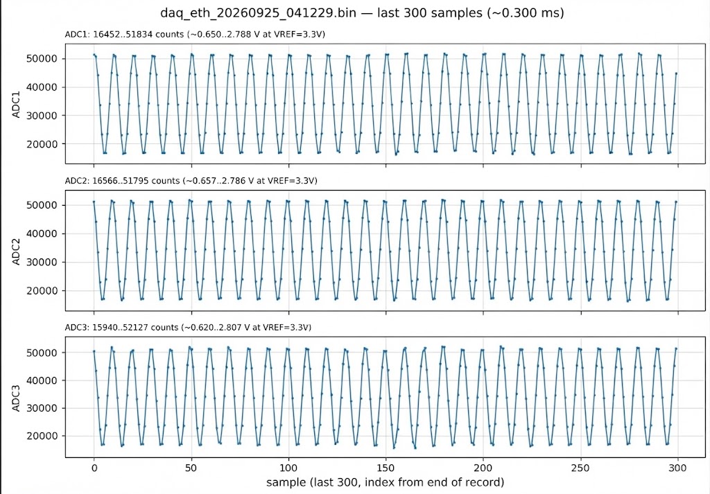
From the daq_eth_20260925_041229.bin capture — the last 300 samples from each ADC show the same periodic input waveform on all three channels.
The plot is primarily used here to verify:
- coherent waveform reconstruction on all three channels;
- correct sample ordering and interleaving;
- absence of visible discontinuities in the displayed window.
Interleaving validation: Three separate buffers deinterleaved into wire format (ch1[i], ch2[i], ch3[i]):
- Samples arrive as triplets in time order
- No duplicate or missing samples in 300-sample window
- Block number matches captured sequence
Throughput Benchmark
The 6 MB/s value is the required acquisition throughput. The benchmark shown below belongs to an earlier test configuration and should not be treated as the current measured Ethernet throughput:
recording=1500 blocks, 5869 rate=6.008 MB/s
blocks=3909 missing=0 bad=0 fragments=11729 rate=6.004 MB/s
blocks=7816 missing=0 bad=0 fragments=23449 rate=6.002 MB/s
blocks=9709 missing=0 bad=0 fragments=29130 rate=6.001 MB/s
This historical benchmark demonstrated:
- ~6.0 MB/s sustained throughput — 512 samples × 3 channels × 2 bytes per sample every 512 µs = 6,000,000 bytes/s
- Zero missing blocks in the shown run under those laboratory conditions
- UDP block fragmentation working — three datagrams per 3072-byte acquisition block (1400 + 1400 + 272 bytes of sample payload)
Lessons Learned
Why Event-Driven?
The biggest win is isolation: ADC ISRs are kept short and bounded, while network transport runs in the main loop. This means:
- Firmware can safely call malloc/pbuf_alloc from the main loop
- LwIP housekeeping cannot disrupt timing capture
- Easy to instrument and debug with UART logging
Buffer Management
A finite queue (128 blocks) is better than infinite:
- Dropped blocks are visible (explicit block number gaps)
- No silent, creeping data corruption
- Receiver knows immediately if the system is backpressured
Memory Layout
The current firmware places ADC DMA buffers in DMA-accessible SRAM and runs with the current no-D-cache configuration:
- ADC DMA buffers are not placed in DTCMRAM
- Ethernet/LwIP buffers use the memory regions required by the current Ethernet configuration
- Cache-maintenance calls must match the actual cache state; the current firmware does not rely on D-cache coherency operations
Interleaving
Samples arrive in three separate DMA buffers but must be interleaved on the wire (ch1[0], ch2[0], ch3[0], …). The interleaving step is performed in the acquisition path; its exact execution time is build- and measurement-dependent and is not assigned a fixed value here.
References & Resources
- STM32H743 Reference Manual (RM0433): ADC, DMA, Ethernet, Timer chapters
- LwIP Documentation: https://savannah.nongnu.org/projects/lwip/
- u-blox NEO-M8T Integration Guide: GNSS timing, PPS output, NMEA parsing
- Ethernet MTU & UDP Fragmentation: RFC 791 (IP), RFC 768 (UDP)
Scalability & Future Work
Multi-Node Array Extension
This single-node DAQ is the building block for distributed arrays. With $N$ synchronized receivers:
Site A (192.168.7.2)    Site B (192.168.7.3)    Site C (192.168.7.4)
    ├─ ADC1, 2, 3           ├─ ADC1, 2, 3           ├─ ADC1, 2, 3
    ├─ NEO-M8T PPS          ├─ NEO-M8T PPS          ├─ NEO-M8T PPS
    └─ Ethernet             └─ Ethernet             └─ Ethernet
              │                      │                      │
              └──────────────────────┼──────────────────────┘
                        Ethernet switch or router
                                    │
                                    ▼
                            Array Processing PC
                        (correlate TDOA across nodes)
Each node streams independently; PC synchronizes via:
- UTC timestamps — all nodes driven by GNSS PPS
- GNSS/PPS alignment — nodes use the PPS sequence and timer anchors to establish a common time reference
- Phase/frequency correction — residual timing and oscillator differences are characterized from the recorded timing metadata
Phase-Coherent Analog Backend
Current setup uses voltage amplifiers (analog preamps with no frequency selectivity). For direction-finding, add:
- Analog bandpass — ~5–30 kHz (VLF band)
- Automatic gain control — track varying signal levels (ionospheric mode changes)
- Frequency mixing — down-convert from RF if using higher-frequency antennas (future 100+ kHz work)
Real-Time Direction Finding (FPGA Pipeline)
A companion FPGA could:
- Receive UDP datagrams (bypass CPU bottleneck)
- Accumulate blocks in circular BRAM (1 ms @ 6 MB/s = 6 kB buffer)
- Compute correlations — 3-channel cross-correlation every 512 µs
- Output bearing stream — Ethernet: bearing angle + confidence metric per block
This would give real-time DoA estimation instead of post-processing, enabling adaptive beam steering or frequency hopping response.
GNSS Augmentation
Next phase integrates NEO-M8T fully:
- UART4 NMEA parsing — extract UTC and DOP metrics
- PPS health monitoring — detect signal loss, multipath effects
- Frequency logging — track crystal drift; generate Allan variance plots
- Redundant timing — fallback to RTC if PPS lost for >10 seconds
Design Innovations & Tradeoffs
Why Event-Driven Over RTOS?
Chosen approach: ISR only queues, main loop dequeues & processes
Alternatives considered:
| Approach | Capture-path isolation | Complexity | Suitability for this prototype |
|---|---|---|---|
| Event-driven (chosen) | High | Low | Good |
| FreeRTOS with semaphores | High | Medium | Possible future option |
| Cooperative multitasking | Medium | Medium | Possible |
| Monolithic ISR | Low | High | Rejected |
The current choice keeps the capture path simple and avoids introducing RTOS task scheduling into the timing-critical path. An RTOS remains a possible future choice if the node grows to require multiple independent real-time services.
Current TIM5 Channel Configuration
The current firmware intentionally uses the direct TIM5 CH1 input:
PA0 / TIM5_CH1
      │
      ▼
   TI1FP1
      │
      ▼
TIM5 external clock mode
The older indirect-TI2 arrangement is no longer part of the current implementation.
The reason is architectural as well as practical: ADC triggering has been separated from TIM5. TIM5 only needs to count the external PA0 timing signal and capture PPS, while TIM3 handles the ADC trigger path independently.
Why 512-Sample Blocks?
Block size is a tradeoff:
| Size | Latency | Queue Depth (65 ms) | Frag. Count | Notes |
|---|---|---|---|---|
| 256 | 256 µs | 256 blocks | 1 | Too few fragments, queue bloat |
| 512 | 512 µs | 128 blocks | 3 | Sweet spot |
| 1024 | 1024 µs | 64 blocks | 5+ | Fewer blocks, more fragments |
| 2048 | 2048 µs | 32 blocks | 6–8 | High latency, fragmentation tax |
512 samples is a practical block size for the current implementation: it gives 512 µs of data per block while keeping the raw payload at 3072 bytes and limiting each block to three UDP datagrams.
Why Circular (not Linear) Queue?
A bounded circular queue avoids dynamic allocation in the acquisition path and lets the ADC continue running even when Ethernet temporarily falls behind.
Circular queue with explicit dropped-block counter is better:
- Receiver sees the loss (block numbering gap)
- System remains stable under overload
- Forces the user to address backpressure, not hide it
Conclusion
This VLF acquisition unit demonstrates a practical architecture for one station in a distributed lightning direction-finding network. The design keeps the timing-critical path small while moving Ethernet transport and further signal processing outside the ADC interrupt context.
The main engineering results are:
- Event-driven acquisition — ADC DMA interrupts only publish completed blocks; transport runs in the main loop
- Hardware PPS capture — the timer peripheral latches the PPS edge without software-dependent timestamp latency
- Extended timebase — a software counter extends the finite-width hardware timer for long acquisition runs
- Explicit loss detection — finite buffering and block numbers expose transport backpressure
- Layered architecture — acquisition, timing, networking, and PC-side processing remain separate
The prototype has demonstrated:
- ✅ 3-channel ADC acquisition at 1 MSPS per channel
- ✅ Ethernet/UDP transport at a stable ~6 MB/s in the laboratory test
- ✅ GNSS PPS capture framework
- ✅ Python-side block reassembly and loss reporting
- ✅ Raw-data export for offline signal processing
Next phases:
- Complete GNSS integration (UART4 NMEA, UTC epoch binding)
- Add multiple-node array support
- Implement real-time DoA on FPGA (future)
- Field trials with distributed VLF antenna arrays
This design is intended as a reusable building block for a network of ground stations: each station can run the same acquisition unit, receive GNSS timing, and forward raw synchronized data to a central processing system. Direction-of-arrival and multi-station time-difference processing are deliberately kept on the PC side so the station firmware remains small and maintainable.